GL4606-D8
GL4606-D8
- 产品详情
- 产品参数
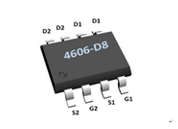
General Description: The GL4606-D8 uses advanced trench technology and design to provide excellent RDS(ON) with low gate charge. It can be used in a wide variety of applications. The package form is SOP-8, which accords with the RoHS standard. Features: N-Channel VDS = 30V,ID = 6.5A RDS(ON) <28mΩ @ VGS=10V RDS(ON) < 58mΩ @ VGS=4.5V ● P-Channel VDS = -30V,ID = -7.0A RDS(ON) < 35mΩ @ VGS=-10V RDS(ON) < 70mΩ @ VGS=-4.5V Low On-Resistance Low Input Capacitance Fast Switching Speed Low Input/Output Leakage |  |
Absolute Maximum Ratings (TA=25℃unless otherwise noted)
Parameter | Symbol | N-Channel | P-Channel | Unit | |
Drain-Source Voltage | VDS | 30 | -30 | V | |
Gate-Source Voltage | VGS | ±20 | ±20 | V | |
Continuous Drain Current | TA=25℃ | ID | 6.5 | -7 | A |
TA=70℃ | 5.4 | -5.8 | |||
Pulsed Drain Current (Note 1) | IDM | 30 | -30 | A | |
Maximum Power Dissipation | TA=25℃ | PD | 2.0 | 2.0 | W |
Operating Junction and Storage Temperature Range | TJ,TSTG | -55 To 150 | -55 To 150 | ℃ |
Thermal Characteristic
Thermal Resistance,Junction-to-Ambient (Note2) | RθJA | N-Ch | 62.5 | ℃/W |
Thermal Resistance,Junction-to-Ambient (Note2) | RθJA | P-Ch | 62.5 | ℃/W |
N-CH Electrical Characteristics (TA=25℃unless otherwise noted)
Parameter | Symbol | Condition | Min | Typ | Max | Unit |
Off Characteristics | ||||||
Drain-Source Breakdown Voltage | BVDSS | VGS=0V ID=250μA | 30 | 33 | - | V |
Zero Gate Voltage Drain Current | IDSS | VDS=30V,VGS=0V | - | - | 1 | μA |
Gate-Body Leakage Current | IGSS | VGS=±20V,VDS=0V | - | - | ±100 | nA |
On Characteristics (Note 3) | ||||||
Gate Threshold Voltage | VGS(th) | VDS=VGS,ID=250μA | 1 | 1.6 | 3 | V |
Drain-Source On-State Resistance | RDS(ON) | VGS=10V, ID=6A | - | 20 | 28 | mΩ |
Forward Transconductance | gFS | VDS=5V,ID=6A | 15 | - | - | S |
Dynamic Characteristics (Note4) | ||||||
Input Capacitance | Clss | VDS=15V,VGS=0V, F=1.0MHz | - | 255 | - | PF |
Output Capacitance | Coss | - | 45 | - | PF | |
Reverse Transfer Capacitance | Crss | - | 35 | - | PF | |
Switching Characteristics (Note 4) | ||||||
Turn-on Delay Time | td(on) | VDD=15V, RL=2.5Ω VGS=10V,RGEN=3Ω | - | 4.5 | - | nS |
Turn-on Rise Time | tr | - | 2.5 | - | nS | |
Turn-Off Delay Time | td(off) | - | 14.5 | - | nS | |
Turn-Off Fall Time | tf | - | 3.5 | - | nS | |
Total Gate Charge | Qg | VDS=15V,ID=6A, VGS=10V | - | 13 | - | nC |
Gate-Source Charge | Qgs | - | 5.5 | - | nC | |
Gate-Drain Charge | Qgd | - | 3.5 | - | nC | |
Drain-Source Diode Characteristics | ||||||
Diode Forward Voltage (Note 3) | VSD | VGS=0V,IS=6A | - | 0.8 | 1.2 | V |
P-CH Electrical Characteristics (TA=25℃unless otherwise noted)
Parameter | Symbol | Condition | Min | Typ | Max | Unit |
Off Characteristics | ||||||
Drain-Source Breakdown Voltage | BVDSS | VGS=0V ID=-250μA | -30 | -33 | - | V |
Zero Gate Voltage Drain Current | IDSS | VDS=-30V,VGS=0V | - | - | -1 | μA |
Gate-Body Leakage Current | IGSS | VGS=±20V,VDS=0V | - | - | ±100 | nA |
On Characteristics (Note 3) | ||||||
Gate Threshold Voltage | VGS(th) | VDS=VGS,ID=-250μA | -1.5 | -1.9 | -2.5 | V |
Drain-Source On-State Resistance | RDS(ON) | VGS=-10V, ID=-6.5A | - | 28 | 33 | mΩ |
Forward Transconductance | gFS | VDS=-5V,ID=-6.5A | 10 | - | - | S |
Dynamic Characteristics (Note4) | ||||||
Input Capacitance | Clss | VDS=-15V,VGS=0V, F=1.0MHz | - | 520 | - | PF |
Output Capacitance | Coss | - | 100 | - | PF | |
Reverse Transfer Capacitance | Crss | - | 65 | - | PF | |
Switching Characteristics (Note 4) | ||||||
Turn-on Delay Time | td(on) | VDD=-15V, RL=2.3Ω VGS=-10V,RGEN=6Ω | - | 7.5 | - | nS |
Turn-on Rise Time | tr | - | 5.5 | - | nS | |
Turn-Off Delay Time | td(off) | - | 19 | - | nS | |
Turn-Off Fall Time | tf | - | 7 | - | nS | |
Total Gate Charge | Qg | VDS=-15V,ID=-6.5A VGS=-10V | - | 9.2 | - | nC |
Gate-Source Charge | Qgs | - | 1.6 | - | nC | |
Gate-Drain Charge | Qgd | - | 2.2 | - | nC | |
Drain-Source Diode Characteristics | ||||||
Diode Forward Voltage (Note 3) | VSD | VGS=0V,IS=-6.5A | - | - | -1.2 | V |
Notes:
Repetitive Rating: Pulse width limited by maximum junction temperature.
Surface Mounted on FR4 Board, t ≤ 10 sec.
Pulse Test: Pulse Width ≤ 300μs, Duty Cycle ≤ 2%.
Guaranteed by design, not subject to production
N- Channel Typical Electrical and Thermal Characteristics (Curves)
Square Wave Pluse Duration(sec)
Figure 13 Normalized Maximum Transient Thermal Impedance
Company:Wuxi Guang Lei electronic technology co., LTD
TEL:13961734102 Mr.yuan